Selected Journal Publications
- "Additive Opto-Thermomechanical Nanoprinting and Nanorepairing under Ambient Conditions", Nano Letters, 20, 5057–5064, (2020). This work is highlighted on Phys.org and Nanowerk.
- "Acoustofluidic Scanning Nanoscope with High Resolution and Large Field of View", ACS Nano, 14, 8624–8633, (2020).
- "Laser additive nano-manufacturing under ambient conditions", Nanoscale, 11, 16187 (2019).
- "Optothermal microbubble assisted manufacturing of nanogap-rich structures for active chemical sensing", Nanoscale, 11, 20589-20597 (2019).
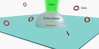
- "Optothermally generated surface bubble and its applications", Nanoscale, 9, 6622 (2017).
- "Practical guide to the realization of a convertible optical trapping system", Optics Express, 25, 2496 (2017)
- "Single-molecule detection at high concentrations with optical aperture nanoantennas", Nanoscale, 8, 9480 (2016).
- "Theory and experiment on particle trapping and manipulation via optothermally generated bubbles", Lab on a Chip, 14, 384 (2014).
- "A reconfigurable plasmofluidic lens", Nature Communications, 4, 2305 (2013).
Full List of Journal Publications
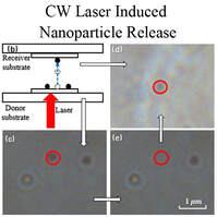
[36] "Determining the laser-induced release probability of a nanoparticle from a soft substrate", Xuesong Gao, Chandu Byram, Jordan Adams, and Chenglong Zhao. Optics Letters 47, 6181-6184 (2022) [PDF]
This Letter presents a study of laser-induced nanoparticle release from a soft substrate in air under different conditions. A continuous wave (CW) laser heats a nanoparticle and causes a rapid thermal expansion of the substrate, which gives an upward momentum that releases the nanoparticle from the substrate. The release probability of different nanoparticles from different substrates under different laser intensities is studied. The effects of surface properties of substrates and surface charges of the nanoparticles on the release are also investigated. The mechanism of nanoparticle release demonstrated in this work is different from that of laser-induced forward transfer (LIFT). Owing to the simplicity of this technology and the wide availability of commercial nanoparticles, this nanoparticle release technology may find applications in nanoparticle characterization and nanomanufacturing.
This Letter presents a study of laser-induced nanoparticle release from a soft substrate in air under different conditions. A continuous wave (CW) laser heats a nanoparticle and causes a rapid thermal expansion of the substrate, which gives an upward momentum that releases the nanoparticle from the substrate. The release probability of different nanoparticles from different substrates under different laser intensities is studied. The effects of surface properties of substrates and surface charges of the nanoparticles on the release are also investigated. The mechanism of nanoparticle release demonstrated in this work is different from that of laser-induced forward transfer (LIFT). Owing to the simplicity of this technology and the wide availability of commercial nanoparticles, this nanoparticle release technology may find applications in nanoparticle characterization and nanomanufacturing.
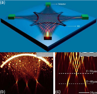
[35] "An acoustofluidic scanning nanoscope using enhanced image stacking and processing", Geonsoo Jin, Joseph Rich, Jianping Xia, Albert J. He, Chenglong Zhao* and Tony Jun Huang*. *Corresponding Authors. Microsystems & Nanoengineering 8, 81 (2022) [PDF]
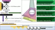
Nanoscale optical resolution with a large field of view is a critical feature for many research and industry areas, such as semiconductor fabrication, biomedical imaging, and nanoscale material identification. Several scanning microscopes have been developed to resolve the inverse relationship between the resolution and field of view; however, those scanning microscopes still rely upon fluorescence labeling and complex optical systems. To overcome these limitations, we developed a dual-camera acoustofluidic nanoscope with a seamless image merging algorithm (alpha-blending process). This design allows us to precisely image both the sample and the microspheres simultaneously and accurately track the particle path and location. Therefore, the number of images required to capture the entire field of view (200 × 200 μm) by using our acoustofluidic scanning nanoscope is reduced by 55-fold compared with previous designs. Moreover, the image quality is also greatly improved by applying an alpha-blending imaging technique, which is critical for accurately depicting and identifying nanoscale objects or processes. This dual-camera acoustofluidic nanoscope paves the way for enhanced nanoimaging with high resolution and a large field of view.
Nanoscale optical resolution with a large field of view is a critical feature for many research and industry areas, such as semiconductor fabrication, biomedical imaging, and nanoscale material identification. Several scanning microscopes have been developed to resolve the inverse relationship between the resolution and field of view; however, those scanning microscopes still rely upon fluorescence labeling and complex optical systems. To overcome these limitations, we developed a dual-camera acoustofluidic nanoscope with a seamless image merging algorithm (alpha-blending process). This design allows us to precisely image both the sample and the microspheres simultaneously and accurately track the particle path and location. Therefore, the number of images required to capture the entire field of view (200 × 200 μm) by using our acoustofluidic scanning nanoscope is reduced by 55-fold compared with previous designs. Moreover, the image quality is also greatly improved by applying an alpha-blending imaging technique, which is critical for accurately depicting and identifying nanoscale objects or processes. This dual-camera acoustofluidic nanoscope paves the way for enhanced nanoimaging with high resolution and a large field of view.
[34] "Intelligent nanoscope for rapid nanomaterial identification and classification", Geonsoo Jin, Seongwoo Hong, Joseph Rich, Jianping Xia, Kyeri Kim, Lingchong You, Chenglong Zhao* and Tony Jun Huang*.
*Corresponding Authors. Lab on a Chip, (2022). DOI: 10.1039/D2LC00206J [PDF]
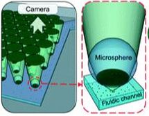
Machine learning image recognition and classification of particles and materials is a rapidly expanding field. However, nanomaterial identification and classification are dependent on the image resolution, the image field of view, and the processing time. Optical microscopes are one of the most widely utilized technologies in laboratories across the world, due to their nondestructive abilities to identify and classify critical micro-sized objects and processes, but identifying and classifying critical nano-sized objects and processes with a conventional microscope are outside of its capabilities, due to the diffraction limit of the optics and small field of view. To overcome these challenges of nanomaterial identification and classification, we developed an intelligent nanoscope that combines machine learning and microsphere array-based imaging to: (1) surpass the diffraction limit of the microscope objective with microsphere imaging to provide high-resolution images; (2) provide large field-of-view imaging without the sacrifice of resolution by utilizing a microsphere array; and (3) rapidly classify nanomaterials using a deep convolution neural network. The intelligent nanoscope delivers more than 46 magnified images from a single image frame so that we collected more than 1000 images within 2 seconds. Moreover, the intelligent nanoscope achieves a 95% nanomaterial classification accuracy using 1000 images of training sets, which is 45% more accurate than without the microsphere array. The intelligent nanoscope also achieves a 92% bacteria classification accuracy using 50 000 images of training sets, which is 35% more accurate than without the microsphere array. This platform accomplished rapid, accurate detection and classification of nanomaterials with miniscule size differences. The capabilities of this device wield the potential to further detect and classify smaller biological nanomaterial, such as viruses or extracellular vesicles.
*Corresponding Authors. Lab on a Chip, (2022). DOI: 10.1039/D2LC00206J [PDF]
Machine learning image recognition and classification of particles and materials is a rapidly expanding field. However, nanomaterial identification and classification are dependent on the image resolution, the image field of view, and the processing time. Optical microscopes are one of the most widely utilized technologies in laboratories across the world, due to their nondestructive abilities to identify and classify critical micro-sized objects and processes, but identifying and classifying critical nano-sized objects and processes with a conventional microscope are outside of its capabilities, due to the diffraction limit of the optics and small field of view. To overcome these challenges of nanomaterial identification and classification, we developed an intelligent nanoscope that combines machine learning and microsphere array-based imaging to: (1) surpass the diffraction limit of the microscope objective with microsphere imaging to provide high-resolution images; (2) provide large field-of-view imaging without the sacrifice of resolution by utilizing a microsphere array; and (3) rapidly classify nanomaterials using a deep convolution neural network. The intelligent nanoscope delivers more than 46 magnified images from a single image frame so that we collected more than 1000 images within 2 seconds. Moreover, the intelligent nanoscope achieves a 95% nanomaterial classification accuracy using 1000 images of training sets, which is 45% more accurate than without the microsphere array. The intelligent nanoscope also achieves a 92% bacteria classification accuracy using 50 000 images of training sets, which is 35% more accurate than without the microsphere array. This platform accomplished rapid, accurate detection and classification of nanomaterials with miniscule size differences. The capabilities of this device wield the potential to further detect and classify smaller biological nanomaterial, such as viruses or extracellular vesicles.
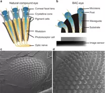
[33] "Biomimetic apposition compound eye fabricated using microfluidic-assisted 3D printing", Bo Dai*, Liang Zhang*, Chenglong Zhao*, Hunter Bachman, Ryan Becker, John Mai, Ziao Jiao, Wei Li, Lulu Zheng, Xinjun Wan, Tony Jun Huang, Songlin Zhuang & Dawei Zhang. * These authors contribute equally. Nature Communications, 12, 6458, (2021). [PDF]
After half a billion years of evolution, arthropods have developed sophisticated compound eyes with extraordinary visual capabilities that have inspired the development of artificial compound eyes. However, the limited 2D nature of most traditional fabrication techniques makes it challenging to directly replicate these natural systems. Here, we present a biomimetic apposition compound eye fabricated using a microfluidic-assisted 3D-printing technique. Each microlens is connected to the bottom planar surface of the eye via intracorporal, zero-crosstalk refractive-index-matched waveguides to mimic the rhabdoms of a natural eye. Full-colour wide-angle panoramic views and position tracking of a point source are realized by placing the fabricated eye directly on top of a commercial imaging sensor. As a biomimetic analogue to naturally occurring compound eyes, the eye’s full-colour 3D to 2D mapping capability has the potential to enable a wide variety of applications from improving endoscopic imaging to enhancing machine vision for facilitating human–robot interactions.
After half a billion years of evolution, arthropods have developed sophisticated compound eyes with extraordinary visual capabilities that have inspired the development of artificial compound eyes. However, the limited 2D nature of most traditional fabrication techniques makes it challenging to directly replicate these natural systems. Here, we present a biomimetic apposition compound eye fabricated using a microfluidic-assisted 3D-printing technique. Each microlens is connected to the bottom planar surface of the eye via intracorporal, zero-crosstalk refractive-index-matched waveguides to mimic the rhabdoms of a natural eye. Full-colour wide-angle panoramic views and position tracking of a point source are realized by placing the fabricated eye directly on top of a commercial imaging sensor. As a biomimetic analogue to naturally occurring compound eyes, the eye’s full-colour 3D to 2D mapping capability has the potential to enable a wide variety of applications from improving endoscopic imaging to enhancing machine vision for facilitating human–robot interactions.
[32] "Additive Opto-Thermomechanical Nanoprinting and Nanorepairing under Ambient Conditions", Md Shah Alam, Qiwen Zhan, and Chenglong Zhao, Nano Letters, 20, 5057–5064, (2020). [PDF]
We demonstrate an opto-thermomechanical (OTM) nanoprinting method that allows us not only to additively print nanostructures with sub-100 nm accuracy but also to correct printing errors for nanorepairing under ambient conditions. Different from other existing nanoprinting methods, this method works when a nanoparticle on the surface of a soft substrate is illuminated by a continuous-wave (cw) laser beam in a gaseous environment. The laser heats the nanoparticle and induces a rapid thermal expansion of the soft substrate. This thermal expansion can either release a nanoparticle from the soft surface for nanorepairing or transfer it additively to another surface in the presence of optical forces for nanoprinting with sub-100 nm accuracy. Details of the printing mechanism and parameters that affect the printing accuracy are investigated. This additive OTM nanoprinting technique paves the way for rapid and affordable additive manufacturing or 3D printing at the nanoscale under ambient conditions.
We demonstrate an opto-thermomechanical (OTM) nanoprinting method that allows us not only to additively print nanostructures with sub-100 nm accuracy but also to correct printing errors for nanorepairing under ambient conditions. Different from other existing nanoprinting methods, this method works when a nanoparticle on the surface of a soft substrate is illuminated by a continuous-wave (cw) laser beam in a gaseous environment. The laser heats the nanoparticle and induces a rapid thermal expansion of the soft substrate. This thermal expansion can either release a nanoparticle from the soft surface for nanorepairing or transfer it additively to another surface in the presence of optical forces for nanoprinting with sub-100 nm accuracy. Details of the printing mechanism and parameters that affect the printing accuracy are investigated. This additive OTM nanoprinting technique paves the way for rapid and affordable additive manufacturing or 3D printing at the nanoscale under ambient conditions.
[31] "Acoustofluidic Scanning Nanoscope with High Resolution and Large Field of View", Geonsoo Jin, Hunter Bachman, Ty Downing Naquin, Joseph Rufo, Serena Hou, Zhenhua Tian, Chenglong Zhao*, and Tony Jun Huang*, ACS Nano, 14, 8624–8633, (2020). [PDF] (* corresponding author)
Optical imaging with nanoscale resolution and a large field of view is highly desirable in many research areas. Unfortunately, it is challenging to achieve these two features simultaneously while using a conventional microscope. An objective lens with a low numerical aperture (NA) has a large field of view but poor resolution. In contrast, a high NA objective lens will have a higher resolution but reduced field of view. In an effort to close the gap between these trade-offs, we introduce an acoustofluidic scanning nanoscope (AS-nanoscope) that can simultaneously achieve high resolution with a large field of view. The AS-nanoscope relies on acoustofluidic-assisted scanning of multiple microsized particles. A scanned 2D image is then compiled by processing the microparticle images using an automated big-data image algorithm. The AS-nanoscope has the potential to be integrated into a conventional microscope or could serve as a stand-alone instrument for a wide range of applications where both high resolution and large field of view are required.
Optical imaging with nanoscale resolution and a large field of view is highly desirable in many research areas. Unfortunately, it is challenging to achieve these two features simultaneously while using a conventional microscope. An objective lens with a low numerical aperture (NA) has a large field of view but poor resolution. In contrast, a high NA objective lens will have a higher resolution but reduced field of view. In an effort to close the gap between these trade-offs, we introduce an acoustofluidic scanning nanoscope (AS-nanoscope) that can simultaneously achieve high resolution with a large field of view. The AS-nanoscope relies on acoustofluidic-assisted scanning of multiple microsized particles. A scanned 2D image is then compiled by processing the microparticle images using an automated big-data image algorithm. The AS-nanoscope has the potential to be integrated into a conventional microscope or could serve as a stand-alone instrument for a wide range of applications where both high resolution and large field of view are required.
[30] "Optothermal microbubble assisted manufacturing of nanogap-rich structures for active chemical sensing", Farzia Karim, Erick S. Vasquez, Yvonne Sun, and Chenglong Zhao, Nanoscale, 11, 20589-20597 (2019). [PDF]
Guiding analytes to the sensing area is an indispensable step in a sensing system. Most of the sensing systems apply a passive sensing method, which waits for the analytes to diffuse towards the sensor. However, passive sensing methods limit the detection of analytes to a picomolar range on micro/nanosensors for a practical time scale. Therefore, active sensing methods need to be used to improve the detection limit in which the analytes are forced to concentrate on the sensors. In this article, we have demonstrated the manufacturing of nanogap-rich structures for active chemical sensing. Nanogap-rich structures are manufactured from metallic nanoparticles through an optothermally generated microbubble (OGMB) which is a laser-induced micron-sized bubble. The OGMB induces a strong convective flow that helps to deposit metallic nanoparticles to form nanogap-rich structures on a solid surface. In addition, the OGMB is used to guide and concentrate analytes towards the nanogap-rich structures for the active sensing of analytes. An active sensing method can improve the detection limit of chemical substances by an order of magnitude compared to a passive sensing method. The microbubble assisted manufacturing of nanogap-rich structures together with an active analyte sensing method paves a new way for advanced chemical and bio-sensing applications.
Guiding analytes to the sensing area is an indispensable step in a sensing system. Most of the sensing systems apply a passive sensing method, which waits for the analytes to diffuse towards the sensor. However, passive sensing methods limit the detection of analytes to a picomolar range on micro/nanosensors for a practical time scale. Therefore, active sensing methods need to be used to improve the detection limit in which the analytes are forced to concentrate on the sensors. In this article, we have demonstrated the manufacturing of nanogap-rich structures for active chemical sensing. Nanogap-rich structures are manufactured from metallic nanoparticles through an optothermally generated microbubble (OGMB) which is a laser-induced micron-sized bubble. The OGMB induces a strong convective flow that helps to deposit metallic nanoparticles to form nanogap-rich structures on a solid surface. In addition, the OGMB is used to guide and concentrate analytes towards the nanogap-rich structures for the active sensing of analytes. An active sensing method can improve the detection limit of chemical substances by an order of magnitude compared to a passive sensing method. The microbubble assisted manufacturing of nanogap-rich structures together with an active analyte sensing method paves a new way for advanced chemical and bio-sensing applications.
[29] "Laser additive nano-manufacturing under ambient conditions", Chenglong Zhao, Piyush J. Shah and Luke J. Bissell, Nanoscale, 11, 16187 (2019). [PDF]
Additive manufacturing at the macroscale has become a hot topic of research in recent years. It has been used by engineers for rapid prototyping and low-volume production. The development of such technologies at the nanoscale, or additive nanomanufacturing, will provide a future path for new nanotechnology applications. In this review article, we introduce several available toolboxes that can be potentially used for additive nanomanufacturing. We especially focus on laser-based additive nanomanufacturing under ambient conditions.
Additive manufacturing at the macroscale has become a hot topic of research in recent years. It has been used by engineers for rapid prototyping and low-volume production. The development of such technologies at the nanoscale, or additive nanomanufacturing, will provide a future path for new nanotechnology applications. In this review article, we introduce several available toolboxes that can be potentially used for additive nanomanufacturing. We especially focus on laser-based additive nanomanufacturing under ambient conditions.
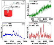
[28] "Print metallic nanoparticles on a fiber probe for 1064-nm surface-enhanced Raman scattering", Ana Sánchez-Solís, Farzia Karim, Md Shah Alam, Qiwen Zhan, Tzarara López-Luke, and Chenglong Zhao, Optics Letters, 44, 4997(2019). [PDF]
This Letter presents 1064-nm surface-enhanced Raman scattering (SERS) on an optical fiber probe, or 1064-nm-SERS-on-fiber. Metallic nanoparticles are printed on an optical fiber probe by using optothermal surface bubbles under ambient conditions. An optothermal surface bubble is a laser-induced micro-sized bubble that is formed on a solid–liquid interface. The SERS activity of the optical fiber probe for 1064-nm Raman microscopy is tested with rhodamine 6G in aqueous solution. The 1064-nm-SERS-on-fiber can reduce the fluorescent background noise that commonly exists in other Raman systems. It can also compensate for the decreased Raman signal due to the use of an infrared Raman laser. The 1064-nm-SERS-on-fiber will find potential applications in low-background-noise biosensing and endoscopy.
This Letter presents 1064-nm surface-enhanced Raman scattering (SERS) on an optical fiber probe, or 1064-nm-SERS-on-fiber. Metallic nanoparticles are printed on an optical fiber probe by using optothermal surface bubbles under ambient conditions. An optothermal surface bubble is a laser-induced micro-sized bubble that is formed on a solid–liquid interface. The SERS activity of the optical fiber probe for 1064-nm Raman microscopy is tested with rhodamine 6G in aqueous solution. The 1064-nm-SERS-on-fiber can reduce the fluorescent background noise that commonly exists in other Raman systems. It can also compensate for the decreased Raman signal due to the use of an infrared Raman laser. The 1064-nm-SERS-on-fiber will find potential applications in low-background-noise biosensing and endoscopy.
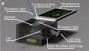
[27] "Colour compound lenses for a portable fluorescence microscope", Bo Dai, Ziao Jiao, Lulu Zheng, Hunter Bachman, Yongfeng Fu, Xinjun Wan, Yule Zhang, Yu Huang, Xiaodian Han, Chenglong Zhao, Tony Jun Huang, Songlin Zhuang & Dawei Zhang.
Light: Science & Applications, 8, 75 (2019). [PDF]
In this article, we demonstrated a handheld smartphone fluorescence microscope (HSFM) that integrates dual-functional polymer lenses with a smartphone. The HSFM consists of a smartphone, a field-portable illumination source, and a dual-functional polymer lens that performs both optical imaging and filtering. Therefore, compared with the existing smartphone fluorescence microscope, the HSFM does not need any additional optical filters.
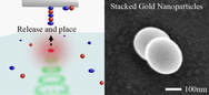
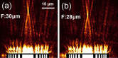
[26] "Nondestructive Approach for Additive Nanomanufacturing of Metallic Nanostructures in the Air" Md Shah Alam, Chenglong Zhao, ACS Omega, 3(1), 1213–1219 (2018). [PDF]
In this article, a mechanism for quick release and transfer of gold nanoparticles (GNPs) from a soft substrate to another substrate under laser illumination is investigated. The heating of GNPs on a soft substrate with a continuous-wave laser causes a rapid thermal expansion of the substrate, which can be used to selectively release and place GNPs onto another surface. In-plane and out-of-plane nanostructures are successfully fabricated using this method. This rapid release-and-place process can be used for additive nonmanufacturing of metallic nanostructures under ambient conditions, which paves a way for affordable nanomanufacturing and enables a wide variety of applications in nanophotonics, ultrasensitive sensing, and nonlinear plasmonics.
In this article, a mechanism for quick release and transfer of gold nanoparticles (GNPs) from a soft substrate to another substrate under laser illumination is investigated. The heating of GNPs on a soft substrate with a continuous-wave laser causes a rapid thermal expansion of the substrate, which can be used to selectively release and place GNPs onto another surface. In-plane and out-of-plane nanostructures are successfully fabricated using this method. This rapid release-and-place process can be used for additive nonmanufacturing of metallic nanostructures under ambient conditions, which paves a way for affordable nanomanufacturing and enables a wide variety of applications in nanophotonics, ultrasensitive sensing, and nonlinear plasmonics.
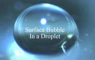
[25] "Fabricated nanogap-rich plasmonic nanostructures through an optothermal surface bubble in a droplet" Farzia Karim, Erick S. Vasquez, Chenglong Zhao, Optics Letters, 43(2), 334 (2018). [PDF]
A rapid and cost-effective method for the fabrication of nanogap-rich structures is demonstrated in this Letter. The method utilizes the Marangoni convection around an optothermal surface bubble inside a liquid droplet with a nanoliter volume. The liquid droplet containing metallic nanoparticles reduces the sample consumption and confines the liquid flow. The optothermal surface bubble creates a strong convective flow that allows for the rapid deposition of the metallic nanoparticles to form nanogap-rich structures on any substrate under ambient conditions. This method will enable a broad range of applications such as biosensing, environmental analysis, and nonlinear optics..
A rapid and cost-effective method for the fabrication of nanogap-rich structures is demonstrated in this Letter. The method utilizes the Marangoni convection around an optothermal surface bubble inside a liquid droplet with a nanoliter volume. The liquid droplet containing metallic nanoparticles reduces the sample consumption and confines the liquid flow. The optothermal surface bubble creates a strong convective flow that allows for the rapid deposition of the metallic nanoparticles to form nanogap-rich structures on any substrate under ambient conditions. This method will enable a broad range of applications such as biosensing, environmental analysis, and nonlinear optics..
[24] "Review of optical detection of single molecules beyond the diffraction and diffusion limit using plasmonic nanostructures" Farzia Karim, Todd B. Smith, Chenglong Zhao, J. Nanophoton. 12(1), 012504 (2017). [PDF]
Single-molecule detection has become a unique and indispensable tool for the study of molecular motions and interactions at the single-molecule level. Unlike ensemble measurement where the information is averaged, single-molecule analysis yields invaluable information on both the individual molecular properties and their microenvironment. Among the various technologies for the detection of single molecules, the detection with optical methods has many advantages in terms of its high sensitivity, electrical passiveness, and robustness. The recent advances in the engineering of either the excitation light or the solution of the molecules have paved the way for enhanced single-molecule detection. We present recent developments and future perspectives for single-molecule detection in the following three regimes: on a dry surface, in solutions at ultralow concentrations, and in solutions at native physiological concentrations.
Single-molecule detection has become a unique and indispensable tool for the study of molecular motions and interactions at the single-molecule level. Unlike ensemble measurement where the information is averaged, single-molecule analysis yields invaluable information on both the individual molecular properties and their microenvironment. Among the various technologies for the detection of single molecules, the detection with optical methods has many advantages in terms of its high sensitivity, electrical passiveness, and robustness. The recent advances in the engineering of either the excitation light or the solution of the molecules have paved the way for enhanced single-molecule detection. We present recent developments and future perspectives for single-molecule detection in the following three regimes: on a dry surface, in solutions at ultralow concentrations, and in solutions at native physiological concentrations.
[23] "Optothermally generated surface bubble and its applications"
Yuliang Xie, and Chenglong Zhao, Nanoscale, 9, 6622 (2017). [PDF] (Invited Review)
Under laser illumination, a solid-state surface or nanostructure can turn into micro/nano heating source with the so-called optothermal effect. This effect allows for non-invasive control of the heat at the micro/nanoscales. In the presence of liquid, a surface bubble can be generated on top of the solid surface or nanostructure at a temperature much higher than the boiling point of the liquid. The high temperature and the fluid flow associated with the optothermally generated surface bubble enable many intriguing applications ranging from the micro/nano-manipulation of fluids, particles, cells, and light to the synthesis of micro/nano-structures under ambient conditions. In this review article, we present the fundamentals, recent developments, and future perspectives in this emerging field.
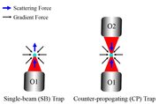
[22] "Practical guide to the realization of a convertible optical trapping system"
Chenglong Zhao, Optics Express, 25, 2496 (2017) [PDF]
In this article, we provide a detailed guide to the construction of a convertible optical trapping system for either single-beam or counter-propagating trap. The single-beam trap maintains all the functionalities that a conventional optical tweezer has. While the counter-propagating trap allows for the trapping of particles that single-beam trap cannot handle. The counter-propagating trap can be easily switched to a single-beam trap, and vice versa. Therefore, this convertible optical trapping system allows for the trapping and manipulation of particles with a wide variety of sizes and materials.

[21] "Single-molecule detection at high concentrations with optical aperture nanoantennas"
Md Shah Alam, Farzia Karim and Chenglong Zhao, Nanoscale, 8, 9480 (2016). [PDF] (Invited Review)
Single-molecule detection has become an indispensable technology in life science, and medical research. In order to get meaningful information on many biological processes, single-molecule analysis is required in micro-molar concentrations. At such high concentrations, it is very challenging to isolate a single molecule with conventional diffraction-limited optics. Recently, optical aperture nanoantennas (OANs) have emerged as a powerful tool to enhance the single-molecule detection under a physiological environment. The OANs, which consist of nano-scale apertures on a metallic film, have the following unique properties: (1) nanoscale light confinement; (2) enhanced fluorescence emission; (3) tunable radiation pattern; (4) reduced background noise; and (5) massive parallel detection. This review presents the fundamentals, recent developments and future perspectives in this emerging field.

[20] "Probing Cell Deformability via Acoustically Actuated Bubbles"
Yuliang Xie, Nitesh Nama, Peng Li, Zhangming Mao, Po-Hsun Huang, Chenglong Zhao, Francesco Costanzo, and Tony Jun Huang, Small 12, 902 (2016). [PDF]
An acoustically actuated, bubble-based technique is developed to investigate the deformability of cells suspended in microfluidic devices. A microsized bubble is generated by an optothermal effect near the targeted cells, which are suspended in a microfluidic chamber. Subsequently, acoustic actuation is employed to create localized acoustic streaming. In turn, the streaming flow results in hydrodynamic forces that deform the cells in situ. The deformability of the cells is indicative of their mechanical properties. The method in this study measures mechanical biomarkers from multiple cells in a single experiment, and it can be conveniently integrated with other bioanalysis and drug-screening platforms. Using this technique, the mean deformability of tens of HeLa, HEK, and HUVEC cells is measured to distinguish their mechanical properties. HeLa cells are deformed upon treatment with Cytochalasin. The technique also reveals the deformability of each subpopulation in a mixed, heterogeneous cell sample by the use of both fluorescent markers and mechanical biomarkers. The technique in this study, apart from being relevant to cell biology, will also enable biophysical cellular diagnosis.
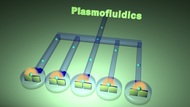
[19] “Plasmofluidics: Merging Light and Fluid at the Micro-/nano-Scale”
Mingsong Wang, Chenglong Zhao, Xiaoyu Miao, Yanhui Zhao, Joseph Rufo, Yanjun Liu, Tony Jun Huang, Yuebing Zheng, Small, 11, 4423 (2015). [PDF] (Invited Review)
Plasmofluidics is the synergistic integration of plasmonics and micro/nanofluidics in devices and applications in order to enhance performance. There has been significant progress in the emerging field of plasmofluidics in recent years. By utilizing the capability of plasmonics to manipulate light at the nanoscale, combined with the unique optical properties of fluids and precise manipulation via micro/nanofluidics, plasmofluidic technologies enable innovations in lab-on-a-chip systems, reconfigurable photonic devices, optical sensing, imaging, and spectroscopy. In this review article, the most recent advances in plasmofluidics are examined and categorized into plasmon-enhanced functionalities in microfluidics and microfluidics-enhanced plasmonic devices. The former focuses on plasmonic manipulations of fluids, bubbles, particles, biological cells, and molecules at the micro/nanoscale. The latter includes technological advances that apply microfluidic principles to enable reconfigurable plasmonic devices and performance-enhanced plasmonic sensors. The article is concluded with perspectives on the upcoming challenges, opportunities, and possible future directions of the emerging field of plasmofluidics.
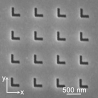
[18] “Coupling between surface plasmon polaritons and transverse electric polarized light via L-shaped nano-apertures”
Jing Yang, Chuang Hu, Qiuling Wen, Chenglong Zhao, and Jiasen Zhang, Optics Letters, 40, 978 (2015). [PDF]
Given that plasmonic fields are intrinsically transverse magnetic (TM), coupling surface plasmon polaritons (SPPs) and transverse electric (TE) polarized light, especially at nanoscale, remain challenging. We propose the use of L-shaped nano-apertures to overcome this fundamental limitation and enable coupling between SPPs and TE polarized light. Polarization conversion originates from the interference of two resonant modes excited in the nano-apertures and the nearly 180° phase retardation between them. The experiments show that both TE-to-plasmon and plasmon-to-TE couplings can be implemented at the subwavelength scale. This discovery provides great freedom when manipulating light based on SPPs at the nanoscale and helps in using the energy of TE polarized light.
[17] “Light Manipulation with Encoded Plasmonic Nanostructures”
Chenglong Zhao, Jiasen Zhang, and Yongmin Liu, EPJ Applied Metamaterials 1, 6 (2014). [PDF] (Invited Review)
Plasmonics, which allows for manipulation of light field beyond the fundamental diffraction limit, has recently attracted tremendous research efforts. The propagating surface plasmon polaritons (SPPs) confined on a metal-dielectric interface provide an ideal two-dimensional (2D) platform to develop subwavelength optical circuits for on-chip information processing and communication. The surface plasmon resonance of rationally designed metallic nanostructures, on the other hand, enables pronounced phase and polarization modulation for light beams travelling in three-dimensional (3D) free space. Flexible 2D and free-space propagating light manipulation can be achieved by encoding plasmonic nanostructures on a 2D surface, promising the design, fabrication and integration of the next-generation optical architectures with substantially reduced footprint. It is envisioned that the encoded plasmonic nanostructures can significantly expand available toolboxes for novel light manipulation. In this review, we presents the fundamentals, recent developments and future perspectives in this emerging field, aiming to open up new avenues to developing revolutionary photonic devices.
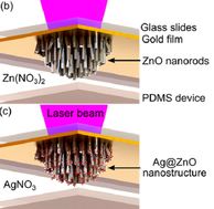
[16] “In-Situ Fabrication of 3D Ag@ZnO Nanostructures for Microfluidic/Surface-Enhanced Raman Scattering (SERS) Systems”.
Yuliang Xie, Shikuan Yang, Zhangming Mao, Peng Li, Chenglong Zhao, Zane Cohick, Po-Hsun Huang, and Tony Jun Huang, ACS Nano. 8, 12175 (2014). [PDF]
In this work, we develop an in situ method to grow highly controllable, sensitive, three-dimensional (3D) surface-enhanced Raman scattering (SERS) substrates via an optothermal effect within microfluidic devices. Implementing this approach, we fabricate SERS substrates composed of Ag@ZnO structures at prescribed locations inside microfluidic channels, sites within which current fabrication of SERS structures has been arduous. Conveniently, properties of the 3D Ag@ZnO nanostructures such as length, packing density, and coverage can also be adjusted by tuning laser irradiation parameters. After exploring the fabrication of the 3D nanostructures, we demonstrate a SERS enhancement factor of up to ∼2 × 10⁶ and investigate the optical properties of the 3D Ag@ZnO structures through finite-difference time-domain simulations. To illustrate the potential value of our technique, low concentrations of biomolecules in the liquid state are detected. Moreover, an integrated cell-trapping function of the 3D Ag@ZnO structures records the surface chemical fingerprint of a living cell. Overall, our optothermal-effect-based fabrication technique offers an effective combination of microfluidics with SERS, resolving problems associated with the fabrication of SERS substrates in microfluidic channels. With its advantages in functionality, simplicity, and sensitivity, the microfluidic-SERS platform presented should be valuable in many biological, biochemical, and biomedical applications.
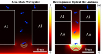
[15] “Single-molecule Detection and Radiation Control in Solutions at High Concentrations via a Heterogeneous Optical Slot Antenna”
Chenglong Zhao, Yongmin Liu, Jing Yang and Jiasen Zhang, Nanoscale, 6, 9103 (2014). [PDF]
We designed a heterogeneous optical slot antenna (OSA) that is capable of detecting single molecule in solutions at high concentrations, where most biological processes occur. The heterogeneous OSA consists of a rectangular nanoslot fabricated on heterogeneous metallic films formed by sequential deposition of gold and aluminum on a glass substrate. The rectangular nanoslot gives rise to large field and fluorescence enhancement for single molecules. The near-field intensity inside a heterogeneous OSA is 170 times larger than that inside an aluminum zero-mode waveguide (ZMW), and the fluorescence emission rate of a molecule inside the heterogeneous OSA is about 70 times higher than that of the molecule in free space. Our proposed heterogeneous optical antenna enables excellent balance between performance and cost. The design takes into account the practical experimental conditions so that the parameters chosen in the simulation are well within the reach of current nano-fabrication technologies. Our results can be used as a direct guidance for designing high-performance, low-cost plasmonic nanodevices for the study of bio-molecule and enzyme dynamics at the single-molecule level.
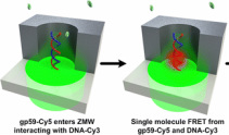
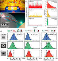
[14] "Dark-Field Illumination on Zero-Mode Waveguide/Microfluidic Hybrid Chip Reveals T4 Protein Interactions"
Yanhui Zhao, Danqi Chen, Hongjun Yue, Michelle M. Spiering, Chenglong Zhao, Stephen J. Benkovic, and Tony Jun Huang, Nano. Lett. 14, 1952 (2014). [PDF]
The ability of zero-mode waveguides (ZMW) to guide light energy into subwavelength-diameter cylindrical nanoapertures has been exploited for single-molecule fluorescence studies of biomolecules at micromolar concentrations, the typical dissociation constants for biomolecular interactions. Although epi-fluorescence microscopy is now adopted for ZMW-based imaging as an alternative to the commercialized ZMW imaging platform, its suitability and performance awaits rigorous examination. Here, we present conical lens-based dark-field fluorescence microscopy, in combination with a ZMW/microfluidic chip, for single-molecule fluorescence imaging. We demonstrate that compared to epi-illumination, the dark-field configuration displayed diminished background and noise, and enhanced signal-to-noise ratios. This signal-to-noise ratio for imaging using the dark-field setup remains essentially unperturbed by the presence of 1 µM background fluorescent molecules. Our design allowed single-molecule FRET studies on revealing weak DNA-protein and protein-protein interactions found with T4 replisomal proteins.
[13] "Theory and experiment on particle trapping and manipulation via optothermally generated bubbles"
Chenglong Zhao*, Yuliang Xie*, Zhangming Mao, Yanhui Zhao, Joseph Rufo, Shikuan Yang, Feng Guo, John D. Mai, and Tony Jun Huang, Lab on a Chip, 14, 384 (2014) . [PDF]
We present a theoretical analysis and experimental demonstration of particle trapping and manipulation around optothermally generated bubbles. We show that a particle located within 500 μm of a surface bubble can be attracted towards a bubble by drag force resulting from a convective flow. Once the particle comes in contact with the bubble's surface, a balance between surface tension forces and pressure forces traps the particle on the bubble surface, allowing the particle to move with the bubble without detaching. The proposed mechanism is confirmed by computational fluid dynamics simulations, force calculations, and experiments. Based on this mechanism, we experimentally demonstrated a novel approach for manipulating microparticles via optothermally generated bubbles. Using this approach, randomly distributed microparticles were effectively collected and carried to predefined locations. Single particles were also manipulated along prescribed trajectories. This bubble-based particle trapping and manipulation technique can be useful in applications such as micro assembly, particle concentration, and high-precision particle separation.
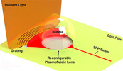
[12] "A reconfigurable plasmofluidic lens"
Chenglong Zhao*, Yongmin Liu*, Yanhui Zhao, Nicholas Fang and Tony Jun Huang
Nature Communications, 4, 2305 (2013). [PDF]
(This work has been highlighted as a News Report on Science Daily, Physics News,
National Science Foundation, Science Codex, Science News, Nano Werk, et al.)
Plasmonics provides an unparalleled method for manipulating light beyond the diffraction limit, making it a promising technology for the development of ultra-small, ultra-fast and power-efficient optical devices. To date, the majority of plasmonic devices are in the solid state and have limited tunability or configurability. Moreover, individual solid-state plasmonic devices lack the ability to deliver multiple functionalities. Here we utilize laser-induced surface bubbles on a metal film to demonstrate, for the first time, a plasmonic lens in a microfluidic environment. Our ‘plasmofluidic lens’ is dynamically tunable and reconfigurable. We record divergence, collimation and focusing of surface plasmon polaritons using this device. The plasmofluidic lens requires no sophisticated nanofabrication and utilizes only a single low-cost diode laser. Our results show that the integration of plasmonics and microfluidics allows for new opportunities in developing complex plasmonic elements with multiple functionalities, high-sensitivity and high-throughput biomedical detection systems, as well as on-chip, all-optical information processing techniques.
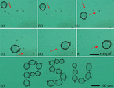
[11] "Optoacoustic tweezers: a programmable, localized cell concentrator based on opto-thermally generated, acoustically activated, surface bubbles"
Chenglong Zhao*, Yuliang Xie*, Yanhui Zhao, Sixing Li, Joseph Rufo, Shikuan Yang, Feng Guo and Tony Jun Huang, Lab on a Chip, 13, 1772 (2013). [PDF]
(This work has been featured as the front cover image on the Journal Lab on a Chip)
We present a programmable, biocompatible technique for dynamically concentrating and patterning particles and cells in a microfluidic device. Since our technique utilizes opto-thermally generated, acoustically activated, surface bubbles, we name it “optoacoustic tweezers”. The optoacoustic tweezers are capable of concentrating particles/cells at any prescribed locations in a microfluidic chamber without the use of permanent structures, rendering it particularly useful for the formation of flexible, complex cell patterns. Additionally, this technique has demonstrated excellent biocompatibility and can be conveniently integrated with other microfluidic units. In our experiments, micro-bubbles were generated by focusing a 405 nm diode laser onto a gold-coated glass chamber. By properly tuning the laser, we demonstrate precise control over the position and size of the generated bubbles. Acoustic waves were then applied to activate the surface bubbles, causing them to oscillate at an optimized frequency. The resulting acoustic radiation force allowed us to locally trap particles/cells, including 15 μm polystyrene beads and HeLa cells, around each bubble. Cell-adhesion tests were also conducted after cell concentrating to confirm the biocompatibility of this technique.
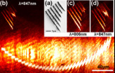
[10] "Flexible wavefront manipulation of surface plasmon polaritons without mechanical motion components"
Chenglong Zhao and Jiasen Zhang, Applied Physics Letters, 98, 211108 (2011). [PDF]
We propose a form of flexible wavefront manipulation of surface plasmonpolaritons (SPPs) without any mechanical motion component. An incoming light pattern, the amplitude of which is modulated by a liquid crystalspatial light modulator, is used to illuminate a grating on an Aufilm acting as a light-SPP coupler. The SPPs launched from the grating have the same intensity distribution as the input light pattern. By changing the input image, continuously variable in-plane SPP focusing on the Aufilm is implemented. The experimental results agree well with numerical simulations.
[9] “Plasmonic Demultiplexer and Guiding”
Chenglong Zhao and Jiasen Zhang, ACS Nano, 4, 6433 (2010). [PDF]
Two-dimensional plasmonic demultiplexers for surface plasmon polaritons (SPPs), which consist of concentric grooves on a gold film, are proposed and experimentally demonstrated to realize light−SPP coupling, effective dispersion, and multiple-channel SPP guiding. A resolution as high as 10 nm is obtained. The leakage radiation microscopy imaging shows that the SPPs of different wavelengths are focused and routed into different SPP strip waveguides. The plasmonic demultiplexer can thus serve as a wavelength division multiplexing element for an integrated plasmonic circuit and also as a plasmonic spectroscopy or filter.
[8] “Binary plasmonics: launching surface plasmon to a desired pattern”
Chenglong Zhao and Jiasen Zhang, Optics Letters, 34, 2417 (2009). [PDF]
We propose a binary plasmonic method to design the binary plasmonic structure (BPS), which is used to launch surface plasmon polaritons (SPPs) to a desired pattern. The BPS is composed of binary pixelated grooves. When a plane wave illuminates the BPS perpendicularly, the relative phases of the launched SPPs are determined by the positions of the grooves, which are designed by a simulated annealing algorithm. Here, we obtain single, three, and five SPP focal spots along the line parallel to the BPS, respectively, and three focal spots, which are located at the apexes of a triangle. The experiment agrees well with the numerical simulation.
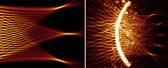
[7] “Focusing surface plasmons to multiple focal spots with a launching diffraction grating”
Chenglong Zhao, Jiayuan Wang, Xiaofei Wu, and Jiasen Zhang, Applied Physics Letters, 94, 111105 (2009). [PDF]
We propose a surface plasmon launching diffraction grating (SPLDG) to obtain multiple focal spots of SPs with nearly equal intensity. The SPLDG is composed of grooves that are located on concentric arcs, whose projections on the chord form a grating. When the incident plane wave illuminates the grating, SPs launched and diffracted into different directions will be approximately focused to multispots on a circle. Here, we obtain three and five focuses and the numerical simulation agrees well with the experiment.
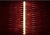
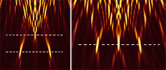
[6] “An experimental study of the plasmonic Talbot effect”, Zhang weiwei, Chenglong Zhao, Jiayuan Wang, and Jiasen Zhang, Optics Express, 17, 19757 (2009). [PDF]
The Talbot effect of the surface plasmon polaritons (SPPs) using SPP launching gratings is studied experimentally. Talbot carpets are obtained and the Talbot distance is given when the paraxial approximation is not satisfied. Multi-layer and multi-level-phase launching gratings are designed to enhance the intensities of the amplitude-modulated revivals. Effective focusing of SPPs with multiple focal spots and a subwavelength full width at half maximum is obtained by using a three-layer four-level-phase launching grating.
The Talbot effect of the surface plasmon polaritons (SPPs) using SPP launching gratings is studied experimentally. Talbot carpets are obtained and the Talbot distance is given when the paraxial approximation is not satisfied. Multi-layer and multi-level-phase launching gratings are designed to enhance the intensities of the amplitude-modulated revivals. Effective focusing of SPPs with multiple focal spots and a subwavelength full width at half maximum is obtained by using a three-layer four-level-phase launching grating.
[5] “Does the leakage radiation profile mirror the intensity profile of surface plasmon polaritons?”, Jiayuan Wang, Chenglong Zhao and Jiasen Zhang, Optics Letters, 35, 1944 (2010). [PDF]
Although the leakage radiation (LR) image intensity is considered to be in proportion to the surface plasmon polariton (SPP) intensity at the metal–air interface, it has not been proven experimentally, to the best of our knowledge. Here we investigate the relationship between the measured LR intensity profile of SPP interference fringes, which are produced by two SPP launching gratings, and the simulated SPP intensity. The experimental modulation depths agree well with the simulation result of the in-plane electric field component of SPPs, which demonstrates that the image intensity in LR microscopy provides the intensity profile of the in-plane component.
Although the leakage radiation (LR) image intensity is considered to be in proportion to the surface plasmon polariton (SPP) intensity at the metal–air interface, it has not been proven experimentally, to the best of our knowledge. Here we investigate the relationship between the measured LR intensity profile of SPP interference fringes, which are produced by two SPP launching gratings, and the simulated SPP intensity. The experimental modulation depths agree well with the simulation result of the in-plane electric field component of SPPs, which demonstrates that the image intensity in LR microscopy provides the intensity profile of the in-plane component.
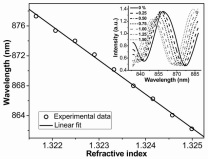
[4] “Refractive index sensor based on surface-plasmon interference”, Xiaofei Wu, Jiasen Zhang, Jianjun Chen, Chenlong Zhao, and Qihuang Gong, Optics Letters 34, 392 (2009). [PDF]
We propose a refractive index sensor based on the interference of two surface-plasmon waves on both surfaces of a gold film with a two-slit structure. The phase of the interference was solved, and the dispersion relation of the real part of Au dielectric function was considered. The sensor was performed with NaCl−H2O solutions of different concentrations and exhibited a linear response and a high sensitivity of 4547 nm/RIU (refractive index unit) to the refractive index change.
We propose a refractive index sensor based on the interference of two surface-plasmon waves on both surfaces of a gold film with a two-slit structure. The phase of the interference was solved, and the dispersion relation of the real part of Au dielectric function was considered. The sensor was performed with NaCl−H2O solutions of different concentrations and exhibited a linear response and a high sensitivity of 4547 nm/RIU (refractive index unit) to the refractive index change.
[3] “Does the leakage radiation profile mirror the intensity profile of surface plasmon polaritons? : reply to comment?”, Jiayuan Wang, Chenglong Zhao and Jiasen Zhang, Optics Letters, 36, 2517 (2011). [PDF]
[2] “The extraordinary radiation pattern of an optical rod antenna”, Chenglong Zhao and Jiasen Zhang, arXiv:1007.2314. [PDF]
[1] "Large-Scale Fabrication of Three-Dimensional Surface Patterns Using Template-Defined Electrochemical Deposition", Shikuan Yang, Michael Ian Lapsley, Bingqiang Cao, Chenglong Zhao, Yanhui Zhao, Qingzhen Hao, Brian Kiraly, Jason Scott, Weizhou Li, Lin Wang, Yong Lei, Tony Jun Huang, Advanced Functional Materials, 23, 720 (2013). [PDF]
*authors with equal contributions.
Note: all of the PDF files linked in this page are copyrighted. They are provided for your convenience, while you can download them only if you are entitled to do so by the corresponding publishers.
Note: all of the PDF files linked in this page are copyrighted. They are provided for your convenience, while you can download them only if you are entitled to do so by the corresponding publishers.
